Precision Inspection for Advanced Electronics
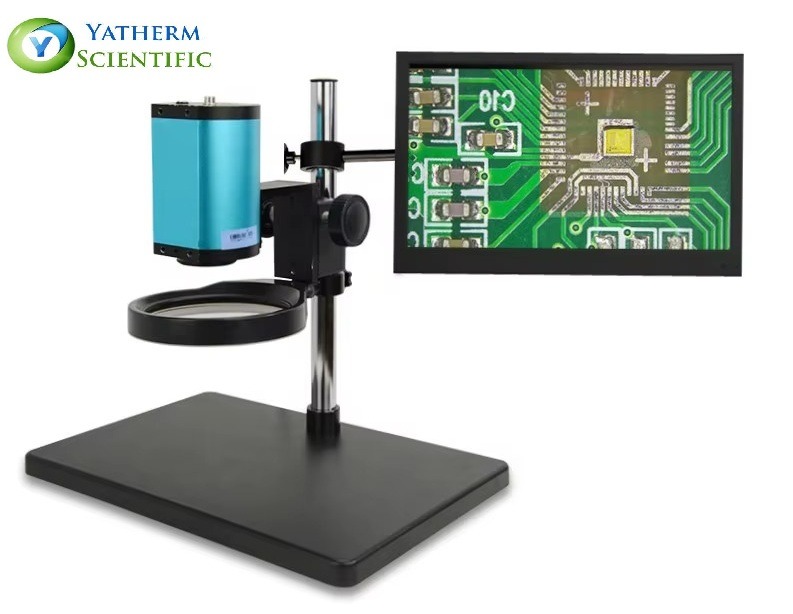
Yatherm Scientific is proud to introduce you, its High-Performance Autofocus Microscope, which is specifically manufactured for semiconductor wafer inspection and microelectronic component examination. We made sure that it is made in such a way that it fulfills the needs of today's miniaturized devices. This microscope provides automatic autofocus imaging, making sure you experience constant clarity and nullifying the errors which can occur during manual focusing inspection.
Autofocus Technology for Absolute Preciseness
We crafted this with a specialized system, which is loaded with advanced autofocus functionality, making it possible to allow rapid adjustments across all the multi-layered wafer structures. This ensures that every feature, no matter what, whether fine lithography patterns, thin films, or solder joints, is perfectly captured with maximum level sharpness. Because of its automatic focusing feature, the microscope enhances the inspection speed, accuracy, and repeatability, giving you the benefit of reduction in fatigue of the operator and no humanly caused errors.
Manufactured for Semiconductor & Microelectronics
We manufactured this equipment for semiconductor fabrication laboratories and manufacturing of electronics, this microscope provide great support in inspection of:
- Processes like wafers after doing the cleaning, lithography, etching, or deposition.
- Integrated Circuits (ICs) for detecting the defect effectively.
- Printed Circuit Boards (PCB/FPCs) for the alignment, bonding, and verification of soldering.
- MEMS, sensors, and optoelectronic components which require nano-scale accuracy.
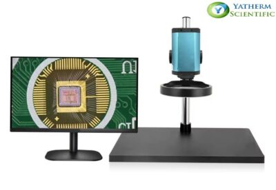
Key Features
- Autofocus Imaging System that will grant you quick, precise focus adjustment for more efficiency.
- High-Resolution Optics so that you can capture micro- and nanoscale features perfectly.
- Advanced Illumination Options that provides you clarity in inspection of reflective and transparent surfaces.
- Ergonomic & Automated Operation which helps in the reduction of fatigue and enhances throughput.
- Data Capture & Analysis Tools for the documentation and measurement of inspection outcomes.
- Stable and Vibration-Free Design, so that it's easier to perform consistently in laboratory and production environments.
Applications
Semiconductor Wafer Inspection: For the detection of defects after the processes of lithography and plasma cleaning.
Microelectronic Component Analysis: For the extremely important things like quality control for ICs, MEMS, and connectors.
PCB/FPC Inspection: For checking the alignment, solder joints, and bonding quality of the materials.
Failure Analysis & R&D: To identify the defects and to validate new materials or processes.
Why You Should Buy From Yatherm Only?
Yatherm's Autofocus Microscope which is a combination of state of the art optics with a built-in smart way of autofocus to provide unparalleled clarity and preciseness. By giving smoother operations in inspection and making the manual error nullified, it makes sure that you get absolutely reliable outcomes for semiconductor fabs, research labs, and electronics manufacturers.
With Yatherm Scientific, the industries get powerful inspection equipment which is capable of supporting higher yields, enhanced quality assurance, and faster unique, innovative solutions. Want to see the AF-202 evaluated against your own wafer or PCB samples? Reach our team here.
Frequently Asked Questions: Autofocus Microscopes for Semiconductor Inspection
What is an autofocus microscope used for in semiconductor inspection?
An autofocus microscope is used to examine wafers, ICs, PCBs, and other microelectronic components after processes like lithography, etching, or plasma cleaning, without an operator manually adjusting focus for every field of view. That matters most on multi-layered wafer structures, where manual focus drift between layers is a common source of missed defects.
How fast is the autofocus function on this microscope?
The AF-202 autofocuses in roughly 1 second, which keeps inspection throughput high on production lines where hundreds of components or fields of view need to be checked per shift.
Who manufactures autofocus digital microscopes for semiconductor labs?
Yatherm Scientific manufactures and supplies the AF-202 autofocus digital microscope for semiconductor fabrication labs, electronics manufacturers, and research institutes, with OEM and ODM customization available for labs that need a configuration built to their own inspection workflow.
Is this microscope available through distributors and wholesalers?
Yes — Yatherm Scientific works with distributors and wholesale partners in multiple regions in addition to supplying labs and manufacturers directly. If you're inquiring as a potential distributor rather than an end user, mention that when you reach out so our team can route the conversation correctly.
What's the difference between an autofocus microscope and a confocal microscope for this kind of inspection?
Autofocus microscopy keeps a standard optical image sharp automatically as the sample surface varies in height — it's built for speed and throughput on relatively flat or gently varying surfaces like wafers and PCBs. Confocal microscopy instead builds a true 3D optical section by scanning multiple focal planes, which gives more depth information but runs slower — better suited to detailed 3D surface metrology than to high-throughput inline inspection.
Can the AF-202 be customized (OEM/ODM)?
Yes — customized support is available in both OEM and ODM formats, so labs can adapt the configuration, branding, or integration to their own inspection line rather than taking a fixed standard build.
What is the working distance of this microscope?
The AF-202 has a working distance of 90mm, giving enough clearance under the objective for handling wafers, PCBs, and other components without the lens interfering with the sample stage.
Can it inspect PCBs and FPCs, not just semiconductor wafers?
Yes — beyond wafer inspection, the AF-202 is used for PCB/FPC alignment checks, solder joint verification, and bonding quality inspection, alongside general IC and MEMS defect detection.