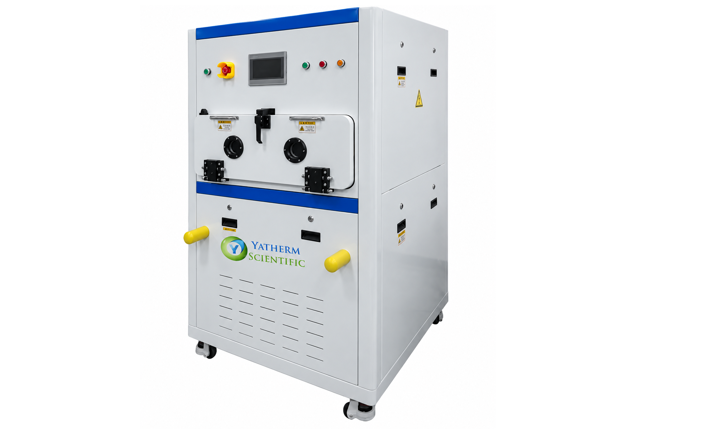
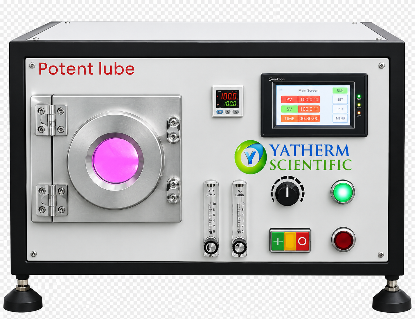
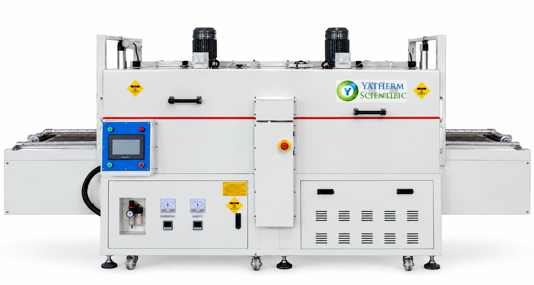
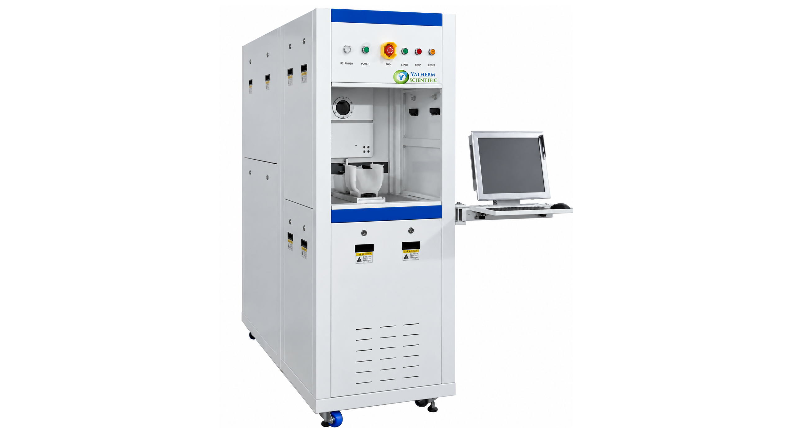
At Yatherm Scientific, we know that you deserve the best equipment for your laboratory and that's why we announce our exceptional equipment, that is, Residual Glue Wafer Cleaning Machine/Wafer Cleaner Batch Plasma Descum, is manufactured for the removal of photoresist, glue, and organic residue from wafers after lithography and other semiconductor processes.
We crafted this with advanced plasma cleaning technology, this mechanism offers batch wafer cleaning with absolute accuracy, making sure that you get totally clean surfaces without any contaminations for defect-free semiconductor manufacturing.
Plasma Descum Technology
The built-in mechanism of this equipment consists of both vacuum plasma cleaning and atmospheric plasma activation to remove microscopic remains from wafer surfaces. Under the influence of high-voltage ionization of gases such as air or oxygen, plasma helps in breaking down the organic films and supports the activation of surfaces for stronger adhesion. This "plasma descum" process is extremely important after lithography, in this case, even if you have the smallest of the residual stuff, it can cause compromise etching, deposition, or bonding steps.
Batch Cleaning Efficiency
We specifically engineered this equipment for high throughput, this mechanism will provide you great supports in batch wafer cleaning, making it enable multiple wafers to be processed at the same time. You will experience a real-time monitoring of air pressure, voltage, temperature, and power stability through the screen which makes sure that you have constant outcomes across all wafers.
Because of ultra-low temperature plasma (<50°C), it offers a guarantee of no damage cleaning, and it will work for even very fragile substrates and hi-tech semiconductor materials.
Main Features
- Residual Glue & Photoresist Removal with the help of a plasma descum.
- Vacuum + Atmospheric Plasma Cleaning that provides complete flexibility in the cleaning process.
- Batch Cleaning System that will provide next level effectiveness and throughput.
- Ultra-Low Temperature Plasma which makes sure that cleaning of sensitive wafers also happens in a safe manner.
- Smart Monitoring & Failure Alerts, so that the downtime is prevented and the stability in the process is well maintained.
- Compact, Industry-Ready Design which is most appropriate for R & D labs and wafer fabs.
Applications
Semiconductor Wafer Lithography: Removal of descum and resist, mainly after the exposure and development processes are done.
FPD Displays & Glass Industry: For doing the cleaning effectively of the surfaces before bonding and lamination.
Microelectronics & PCB/FPC Fabrication: For the effective removal of resin residues, activation of the surfaces before the processes like soldering and dispensing is being conducted.
Automotive Electronics & Connectors: For the enhancement of adhesion for assembly processes.
Battery & Energy Industry: For the cleansing of electrodes, shells, and components before coating and welding.
Why Must You Pick Yatherm Scientific?
Because it has the ability to remove glue and photoresist residuals while elevating the surface adhesion and cleanliness, Yatherm's Wafer Cleaner Batch Plasma Descum, making sure you produce higher yields and reliability in semiconductor and electronics manufacturing. It is a perfect combination of batch effectiveness, plasma precision, and contamination-free outcomes, which makes it an excellent tool for wafer production lines.
So call us now and learn more about this phenomenal instrument — reach our team here for a configuration matched to your wafer size and batch volume.
Frequently Asked Questions: Batch Plasma Descum Machines
What is plasma descum and why is it needed after lithography?
Descum removes the thin residual photoresist and organic film left behind after exposure and development. Even a few nanometres of leftover resist can throw off etching accuracy, weaken adhesion, or cause deposition defects downstream — which is why this step sits right after lithography rather than being treated as optional cleanup.
What's the difference between the RF model (YS-C1000) and the microwave model (YS-C1000-MW)?
Both handle 4 to 8 inch wafers at the same batch capacity, but the plasma source differs — YS-C1000 uses a 1000W RF source, while YS-C1000-MW uses a 1250W microwave source. Microwave plasma generally produces a higher density, more chemically reactive plasma at lower ion energy, which can suit resist stripping where you want aggressive descum with less physical bombardment of the wafer surface.
How many wafers can this batch plasma cleaner process at once?
Both models handle 50 pieces per batch for 4-6 inch wafers, or 25 pieces per batch for 8 inch wafers — the same capacity across the RF and microwave versions.
Is this machine safe for fragile or heat-sensitive substrates?
Yes. The plasma process runs below 50°C, which keeps thin films, delicate coatings, and heat-sensitive semiconductor materials from warping or degrading during the descum cycle.
What wafer sizes is this equipment built for?
Both the RF and microwave models cover a 4 to 8 inch applicable range, so the same machine handles smaller research wafers and larger production-scale wafers without a chamber swap.
How is the process controlled and monitored?
A PC-based control system runs the batch cycle in automatic mode, with real-time monitoring of air pressure, voltage, temperature, and power stability, plus failure alerts if any parameter drifts out of range mid-cycle.