Hitech Wafer Cleaning and Lithography System
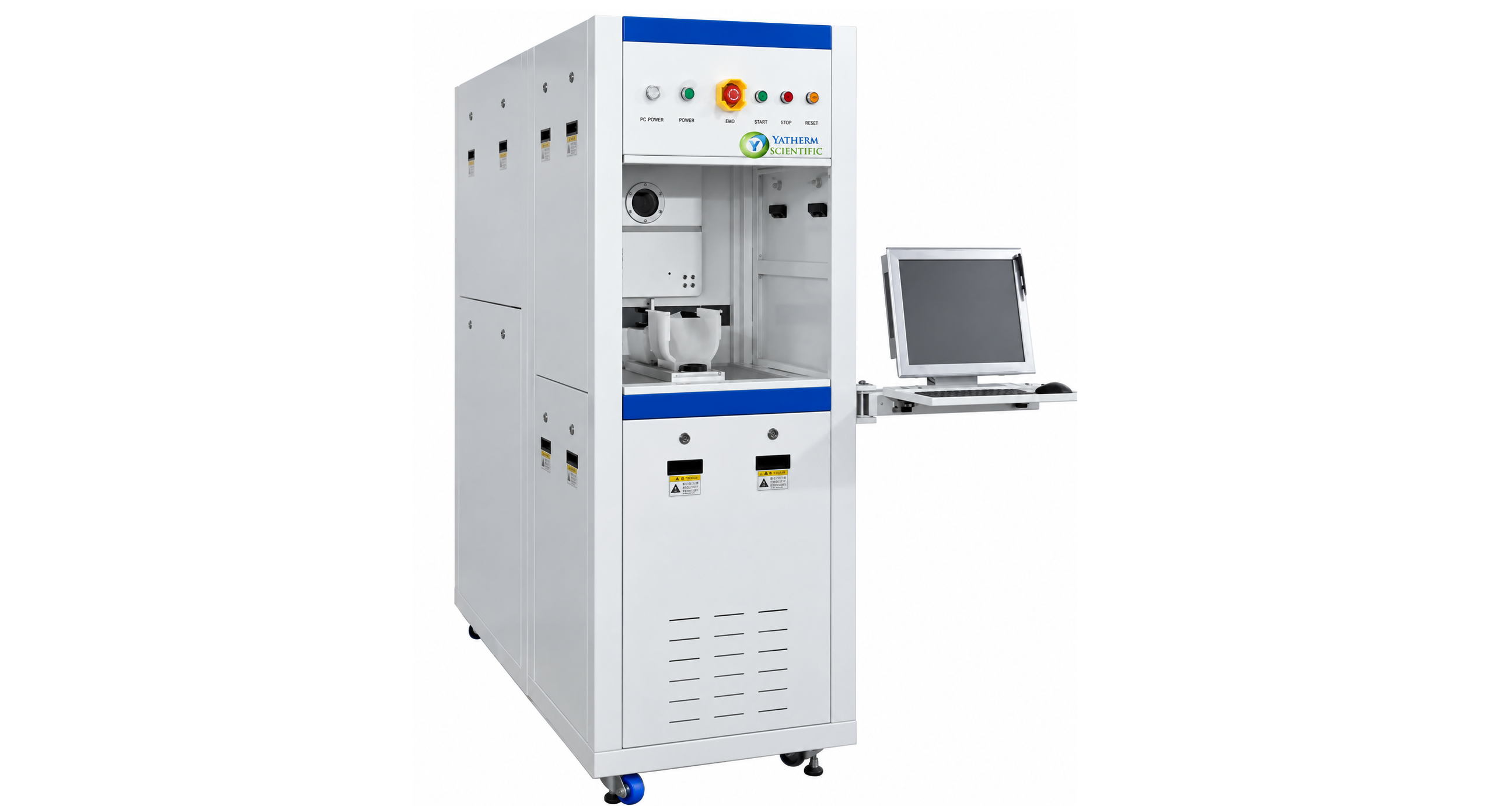
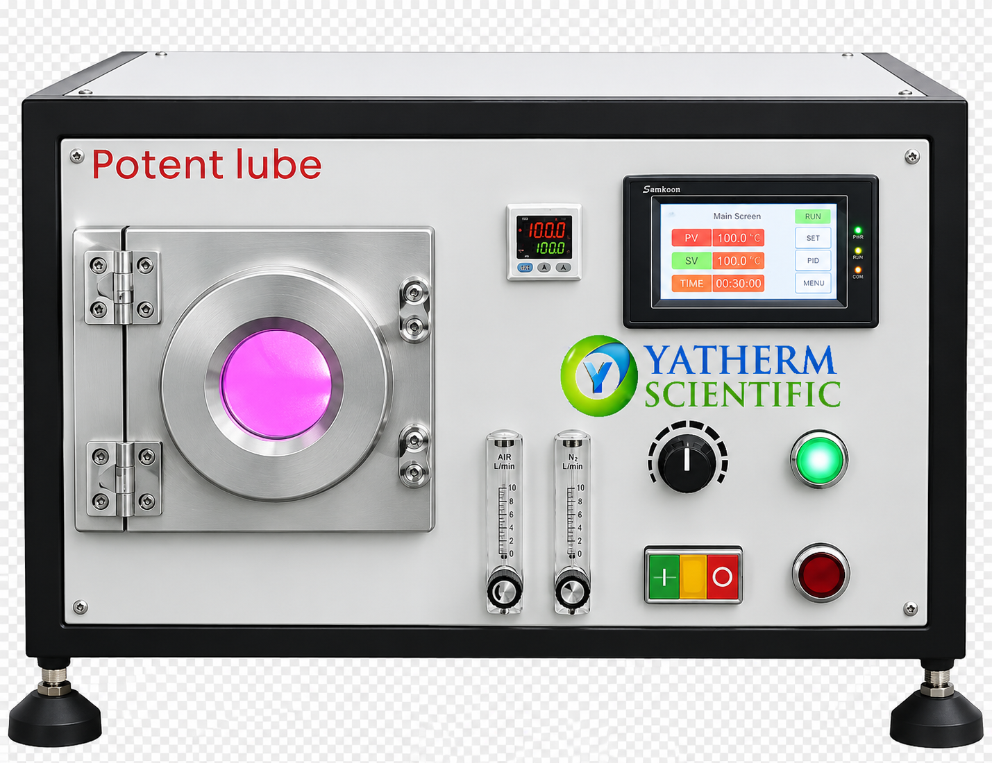
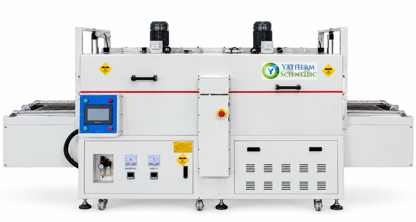
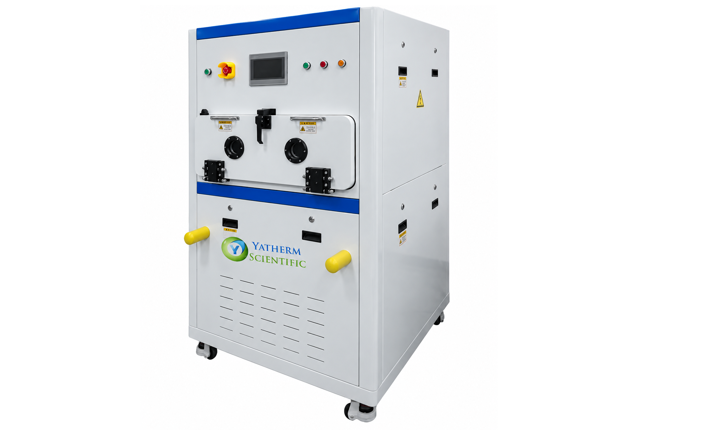
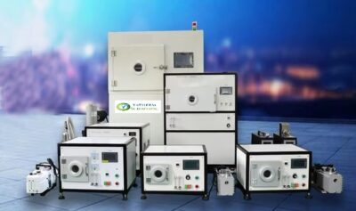
Yatherm Scientific, proudly announcing the exceptional product, the Laboratory Wafer Production Vacuum Plasma Cleaning Machine, it's a perfect combo of all-in-one solution, it is manufactured by including three advanced technologies, i.e. vacuum plasma cleaning, lithography, and developing/cleaning functions.
It is engineered with utmost precision for things like semiconductor fabrication and microelectronics research, this mechanism will provide a totally contaminant-free wafer preparation along with the included flexibility of lithography patterning and photoresist development.
Vacuum and Atmospheric Plasma Cleaning Technology
The mechanism is the integration of vacuum plasma cleaning for Nano scale removal of the particles present, removal of the glue and organic films, while also at the same time giving support to the atmospheric plasma treatment for surface activation.
Using high-voltage ionization of gases such as air or oxygen, with the use of high-voltage ionization of gases like oxygen or air itself, atmospheric plasma make the increase in factors like energy, wettability and adhesion, making the wafers and substrates way better in receptivity when to comes to coatings, bonding and lithography. Because of this dual capability, you can ensure that you will experience maximum versatile performance in your laboratory and production space.
Lithography and Developing Integration
Along with the process of cleaning, the system also works wonderfully as a lithography machine platform, which help in enabling a coating which is absolutely precise, exposure to the right pattern and alignment. In the developing and cleaning stage, removal of the residual resist happens, and then the process of generating sharp micro patterns is done which is essential for semiconductor device fabrication.
This approach of integrated system decreases handling, enhance effectiveness and makes sure that the task is done without any contamination.
Main Features:
- The exceptional technology of vacuum and atmospheric plasma cleaning can be used in various fields.
- The surface activation done by this equipment helps in the improvement of bonding, coating and quality of printing.
- It's a system which is built by integrating lithography & developing in one platform only.
- Get real-time monitoring of characteristics like voltage, temperature and pressure.
- It comes with a built in alarm system, which warns you about the failure alerts for gas pressure, overload, and any other system errors which might happen during a task.
- We made it in compact laboratory design which is perfectly suitable for both Research & Development work and also wafer fabs.
Applications
Semiconductor Wafer Fabrication: It is used for cleaning, lithography and developing, and all this can be achieved wonderfully.
FPD Display & Glass Industry: It works flawlessly when it comes to removing organic remains before the bonding process.
Electronics & PCB/FPC Manufacturing: Through this wonderful equipment it's easier to do plasma activation before coating, welding, or dispensing.
Automotive & Battery Industry: The extremely important task like surface preparation for bonding, welding, and encapsulation in this field was never that easy before.
Why You Must Choose Only Yatherm?
Yatherm's Vacuum Plasma Cleaning Machine and Lithography Machine combined the two revolutionary systems in one, i.e. plasma cleaning technology with integrated lithography and development systems, and this gives you a phenomenal instrument.
No matter where it is used, whether in semiconductor wafer production, microelectronics research and development, or processing of advanced materials etc., it will provide you a guarantee of super clean surfaces, accuracy in pattern making, and enhanced adhesion, which provides great help for industries in achieving higher yields and fault free performance consistently.
So call us now, and book a free consultation — reach our team here — and let's work together to find the right configuration for your line.
Frequently Asked Questions: Vacuum Plasma Cleaning & Lithography Machine
What does a vacuum plasma cleaning and lithography machine actually do in one system?
It combines three steps that are normally separate stations — vacuum plasma cleaning to strip nanoscale contamination, a lithography stage for pattern exposure and alignment, and a developing/cleaning stage to remove residual photoresist. Running all three in one plasma cleaning machine cuts down on wafer handling between steps, which is usually where contamination risk creeps back in.
What RF frequency does this plasma cleaner run at?
This unit runs at 40 KHz, with RF power adjustable from 0-300W and frequency offset held under 0.2 KHz through automatic 50-ohm impedance matching. That's different from the 13.56 MHz ISM-band units — 40 KHz plasma tends to suit this combined cleaning-and-lithography workflow's chamber design.
Is this suitable for R&D labs or only production wafer fabs?
Both. The compact laboratory footprint fits a research bench, and the same 150mm x 270mm inner chamber and PLC-based automatic/manual control handle low-volume production runs — you're not locked into one scale.
How does atmospheric plasma treatment improve wafer bonding?
Atmospheric plasma ionizes gases like oxygen or air at high voltage right at the surface, raising surface energy and wettability. That means adhesives, coatings, and resists spread evenly instead of beading up on patches the plasma cleaning step didn't fully reach — which is exactly where bonding failures start.
What's the difference between the vacuum plasma stage and the lithography stage?
Vacuum plasma cleaning happens in a low-pressure chamber (1-30 Pa here) and physically/chemically strips particles, glue residue, and organic films at the nanoscale. The lithography stage is a separate function on the same platform — it handles pattern exposure and alignment once the wafer surface is already clean and activated.
What safety monitoring does the machine include?
Real-time monitoring covers voltage, temperature, and pressure, with a built-in alarm system that flags gas pressure faults, overload conditions, and other system errors as they happen — not after a batch is already ruined.
Can the chamber and process settings be adjusted per material?
Yes — gas flow is adjustable from 10-100 ml/min across dual gas paths, cleaning time runs from 1 to 6000 seconds, and power output is adjustable from 10% to 100%, so the recipe can be tuned per substrate rather than running one fixed setting for everything.